


A Guide to Printed Circuit Boards (PCBs)
Published date: 12 September 2024
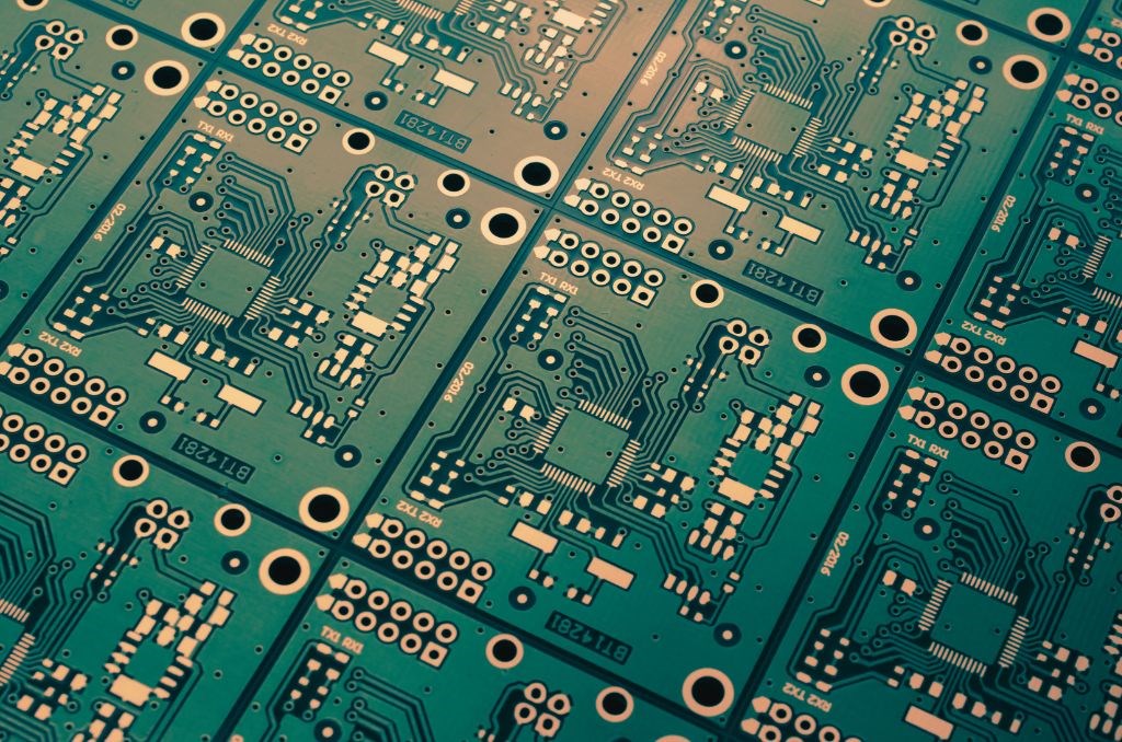
Short for Printed Circuit Board, a PCB is a flat board that provides mechanical support and electrically connects various electronic components. These boards are the backbone of most modern electronics, from smartphones and laptops to industrial machinery and medical devices. If you're curious about how they work, you’ve come to the right place! This guide will walk you through the basics of PCBs, including their design, components, and the assembly process.
What is a PCB?
A printed circuit board (PCB) is an essential part of nearly all electronic devices. Its main function is to provide a platform to mount and connect components like resistors, capacitors, diodes, and integrated circuits. A PCB circuit board ensures that each of these components is arranged in a way that allows the entire system to function properly. Thanks to PCBs, manufacturers can produce electronics that are compact, efficient, and durable.
You'll find PCBs everywhere, from basic home appliances to the most sophisticated aerospace technology. Whether you're looking at a simple toy or a complex computer, chances are there's a PCB inside making everything work.
Fundamentals of PCB Design
When it comes to PCB board design, there are three main types to be aware of, each serving different purposes.
- Single-sided PCBs: These have a single layer of conductive material on one side of the board. They're often used in simple electronics like calculators and radios.
- Double-sided PCBs: These have conductive material on both sides of the board, with components on both the top and bottom. They're used in devices requiring more complex circuits, such as power supplies.
- Multi-layer PCBs: These boards have multiple layers of conductive material separated by insulation. They’re common in high-performance electronics like computers and smartphones, where space is limited, but complex circuits are required.
The key to successful PCB design is ensuring all components are properly positioned to allow the circuit to function as intended. PCB layout and design tools are used to create detailed blueprints that manufacturers follow during production.
PCB Materials
The most widely used base material for PCBs is FR-4, a glass-reinforced epoxy laminate known for its strength, electrical insulating properties and resistance to heat. However, for certain specialised applications, materials like polyimide or ceramic are also used. Conductive materials are utilised to create the electrical connections between the components on a printed circuit board. Copper is the most common choice because of its outstanding electrical conductivity and ease of use; other conductive materials like gold, silver, and indium can also be found in specific designs.
PCB Board Components and Their Placement
A printed circuit board consists of various components, each serving a unique function within the circuit. Some of the most common PCB board components include:
- Resistors: Control the flow of electrical current.
- Capacitors: Store and release electrical energy.
- Diodes: Allow current to flow in one direction.
- Integrated Circuits (ICs): Contain multiple miniaturised circuits within a single package.
PCB components fall into two main categories: through-hole components and surface-mount components. Through-hole components have metal leads that pass through small holes drilled into the PCB and are soldered on the opposite side of the board. On the other hand, surface-mount components are directly placed onto the surface of the board and soldered in place.
PCB Assembly Process
Once the PCB design is finalised, the manufacturing process begins. Here’s a brief look at the main steps:
- Etching: The copper layers on the board are etched away to leave behind the traces that will connect the components.
- Drilling: Holes are drilled for through-hole components or vias that allow for connections between layers on multi-layer PCBs.
- Component Placement: Components are placed onto the PCB by automated machines through either surface mount technology (SMT) or through-hole mounting (THM).
- Soldering: After placement, the components are soldered to secure them in place and create electrical connections. This can be done through wave soldering or reflow soldering techniques.
Once the assembly process is finished, all that’s left to do is to program the circuits and test the completed circuit board.
PCB Coating
To protect the PCB from mechanical stress, as well as environmental factors like moisture, dust, and chemicals, a PCB coating can be applied. Known as conformal coatings, these protective layers form a thin, insulating barrier that preserves the circuit’s integrity. Different types of coatings are available, including acrylic resin, epoxy and silicone resin. In addition to environmental and mechanical protection, specific coatings can offer electrostatic discharge (ESD) protection and help with heat dissipation. Coating helps to extend the lifespan of the PCB, ensuring reliable performance in various conditions.
Grasping the fundamentals of a printed circuit board is key to understanding the technology that powers modern life. From the initial PCB design to component placement and the final PCB board assembly, each step is essential in creating a reliable and efficient electronic product. Whether you're curious about what is a PCB or interested in learning more about PCB board components and PCB coatings, mastering these essentials will help you unlock the full potential of today’s electronic devices.
At Conro we’ll show you how to improve product reliability while increasing performance and lowering costs. Our team of technical support specialists will provide your company with dependable global supply, unrivalled efficiency, and superior technical support. Feel free to contact us on 0208 953 1211 or send us an email to info@conro.com
Comments
There are currently no comments, be the first to comment.